A wafer can be fully fabricated at TSMC's Fab 21 in Arizona, loaded onto a plane, and flown across the Pacific to Taiwan — where it is finally diced, tested, and packaged into a chip you can actually solder onto a board. That round trip is the most concise illustration of America's semiconductor blind spot. The United States poured CHIPS-era capital into the front end of chipmaking — lithography, the wafer fabs themselves — and left the back end, where wafers become usable devices, overwhelmingly offshore.
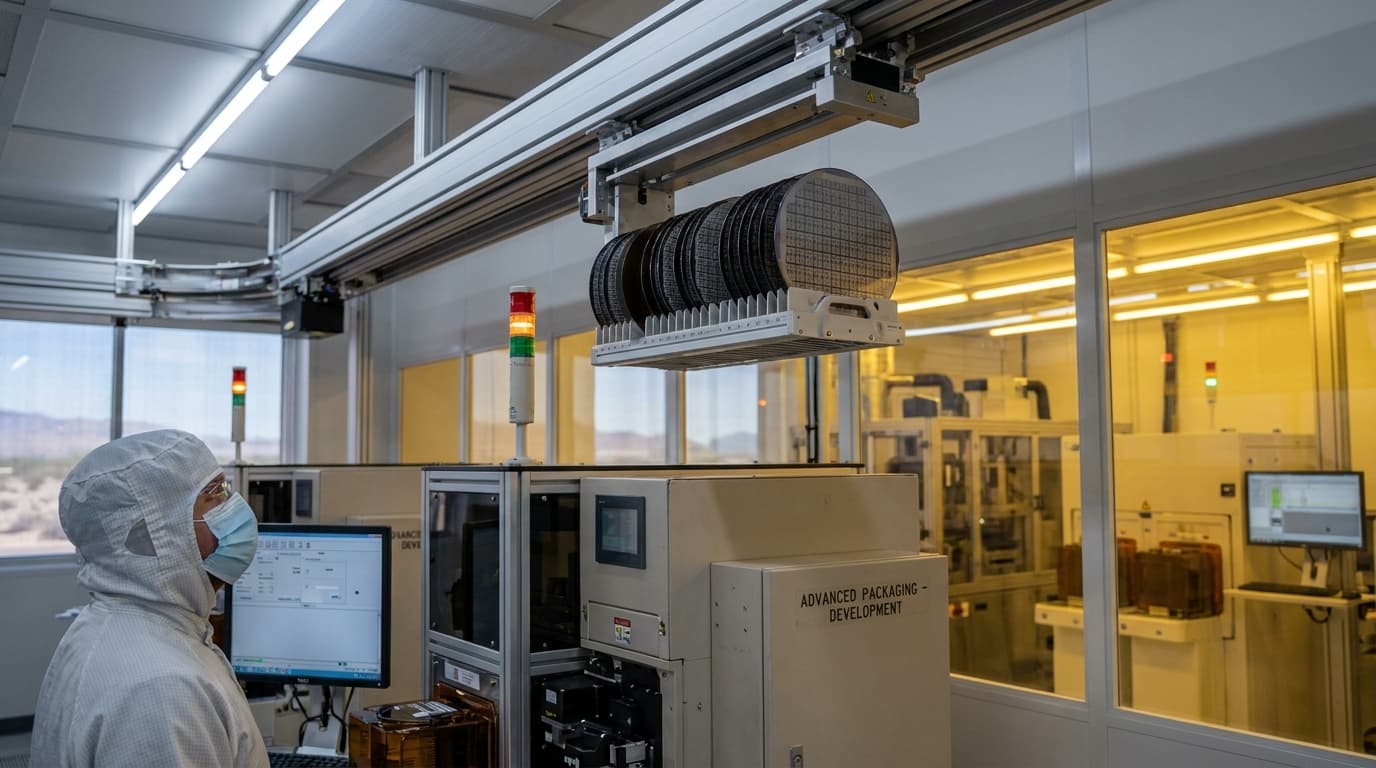
The industry calls the back end OSAT: outsourced semiconductor assembly and test. It is unglamorous compared with extreme-ultraviolet lithography, but it is no longer optional infrastructure. As advanced packaging becomes the bottleneck on AI accelerator output, the geography of assembly and test is becoming the geography of who can actually ship chips.
The numbers: fabs at home, assembly abroad
Market-research estimates for 2025 put Asia-Pacific at roughly 74% of the OSAT market, with North America at about 15%, Europe near 8%, and the Middle East and Africa around 3%. In other words, even after years of reshoring rhetoric, three-quarters of the world's chip assembly and test capacity sits in Asia.
That concentration is not an accident — it is what the incentives bought. CHIPS Act dollars favored wafer fabrication, the capital-intensive, politically marquee end of the business. Packaging, assembly, and test received comparatively little attention even though they are the steps that turn a fabricated wafer into a finished product. The result is a structural mismatch: the U.S. can increasingly make wafers domestically, but it cannot yet finish them at scale on home soil.
The practical consequence is the air-freight loop described above. Because the domestic back end is thin, TSMC's Arizona wafers are currently shipped to Taiwan for dicing, test, and packaging. Arizona-made silicon is, for now, not truly "100% American" — it is American until the wafer is done, then it becomes a Taiwanese finishing job.
Amkor's Peoria campus: the domestic answer
The marquee attempt to close that gap broke ground in Peoria, Arizona, in October 2025. Amkor Technology, one of the world's largest OSAT providers, expanded its planned investment there to $7 billion across two phases — up from an originally announced $2 billion. The U.S. Commerce Department had previously proposed up to $400 million in CHIPS Act funding for the project.
The anchor customers tell the strategic story. Apple is named as the campus's first and largest customer; Nvidia is also an anchor. Apple silicon fabricated at TSMC's nearby Arizona fabs is intended to be packaged and tested by Amkor down the road — a domestic, end-to-end Arizona supply chain on paper. Completed across both phases, the campus is slated to offer more than 750,000 square feet of cleanroom space and as many as 3,000 jobs.
The catch is the calendar. Construction of the first manufacturing facility is expected to complete in mid-2027, with production beginning in early 2028. The most important domestic packaging investment in the country is, in other words, more than two years from shipping its first finished chip.
Why the timing matters: the CoWoS bottleneck
That early-2028 gap collides with the defining supply constraint of the current AI buildout. CoWoS — Chip-on-Wafer-on-Substrate — is the advanced packaging technology that Nvidia and other AI-chip makers depend on to integrate logic and high-bandwidth memory. It has been the primary bottleneck on AI chip output, with TSMC's Taiwan packaging plants reported running near full capacity through 2025.
This reframes the entire reshoring conversation. For the most valuable chips in the market right now, the binding constraint is not lithography — it is packaging. A fab can produce logic wafers, but if there is no CoWoS line to package them, the finished accelerators do not ship. Building wafer fabs in Arizona without a matching back end does not relieve that bottleneck; it relocates only the first half of the process while the choke point stays in Taiwan.
Structural constraints beyond the groundbreaking
Even with Amkor's campus underway, the back end will not snap into place by 2028. Advanced packaging depends on substrate and interposer supply chains, specialized materials, and a deep pool of skilled packaging talent — and those remain concentrated in Asia. Substrate and interposer lead times, materials availability, and a thin domestic packaging workforce are structural constraints, not problems a single groundbreaking solves.
Packaging is a different industrial discipline from wafer fabrication, with its own equipment, process know-how, and supplier ecosystem. Standing up a campus is the visible part; building the surrounding supply web and the trained workforce to run it is the slower, harder part.
TSMC's parallel move toward "all-American" chips
Amkor is not the only player trying to close the loop. TSMC is reportedly accelerating its own Arizona advanced packaging capability, with an in-state packaging facility expected around the end of 2027. Reports describe a much larger ambition — plans cited for multiple fabs and packaging plants in Arizona, including reporting of as many as 12 fabs and four packaging facilities tied to a large planned U.S. investment.
If TSMC's in-state packaging comes online around the end of 2027 and Amkor's lines start in early 2028, Arizona could finally support genuinely "all-American" chips — wafers fabricated and finished without the trans-Pacific detour. But that is a 2027–2028 outcome at the earliest, and it assumes the construction and ramp timelines hold.
Operator and investor takeaway
The strategic conclusion is straightforward: for the highest-value end of the market, packaging — not lithography — is becoming the binding constraint on shipped chips. Domestic wafer capacity is necessary but not sufficient. Until the back end scales, U.S. fab output remains tethered to Asian assembly and test, and the AI accelerator supply chain runs through Taiwanese CoWoS lines regardless of where the wafers were made.
What to watch through 2027 and 2028: whether Amkor's mid-2027 construction completion and early-2028 production start hold; whether TSMC's end-of-2027 in-state packaging target slips; how quickly domestic substrate, interposer, and materials supply can be sourced rather than imported; and whether a U.S. packaging workforce can be trained fast enough to run the new cleanrooms. Each of those is a more reliable signal of reshoring progress than another fab groundbreaking. The fabs were the easy part. The back end is the test.
Related reading
-
[The 48D Cliff: Why Chipmakers Are Racing to Pour Concrete Before Dec. 31, 2026](/article/48d-cliff-chipmakers-racing-pour-concrete-december-2026)
-
[Texas Instruments' $11B Lehi Fab Ramps in 2026 — Straight Into a Mature-Node Glut It Can't Out-Run](/article/texas-instruments-lehi-fab-2026-mature-node-glut)
-
[Samsung's $44B Taylor Fab Slips 2nm Mass Production to 2027 — An Order-Book Problem, Not a Construction One](/article/samsung-taylor-fab-2nm-mass-production-2027-order-book)