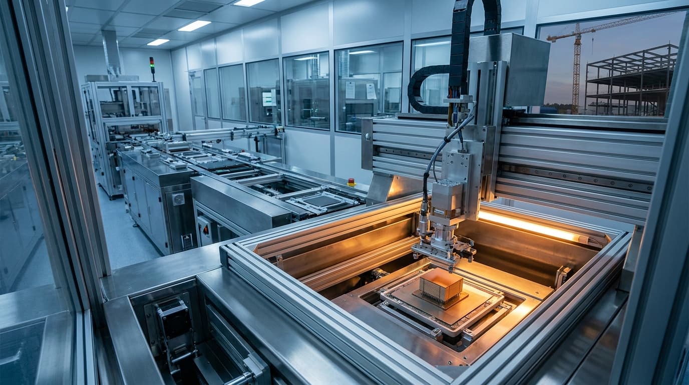
SK hynix broke ground on August 27, 2026 at Purdue Research Park in West Lafayette, Indiana, on what the company describes as the first HBM advanced packaging facility in the United States. The topline number is more than $4 billion — 5.52 trillion won. The site is 540,000 square meters of land owned by Purdue University. Indiana Governor Mike Braun attended. CEO Kwak Noh-Jung told CNBC the site would be a key memory production base in America by 2030.
Two facts from that same announcement belong directly alongside the framing. The plant will not fabricate a wafer. And the first high-bandwidth memory stack packaged in Indiana is currently scheduled for the third quarter of 2029.
Neither is a criticism of the investment, which is real, large, and useful. Both are load-bearing for anyone — a hyperscaler buyer, an Indiana taxpayer, a supplier planning a Midwest footprint — trying to work out what this facility does and when.
What was actually announced
Per Purdue's own release and the company's groundbreaking remarks, the scope is:


Photo: nist.gov
-
Investment: more than $4 billion (5.52 trillion won). The original April 2024 commitment and the federal award documentation both cite $3.87 billion.
-
Site: 540,000 m² (~54 hectares, ~133.5 acres) inside Purdue Research Park, on Purdue-owned land. Indiana won the project over Arizona and Michigan.
-
Scope: back-end only. Advanced DRAM wafers are produced in South Korea and shipped to Indiana for stacking, advanced packaging, and test before finished HBM goes to US customers. There is no front-end wafer fab in the plan.
-
Timeline: cleanroom completion targeted October 2028; mass production targeted Q3 2029. TrendForce reports the launch product is HBM4E.
-
Employment: roughly 1,000 direct facility jobs at full operation plus hundreds of construction jobs, per NIST. Korean coverage cites a broader ~7,000 figure spanning direct, indirect, construction and local supply-chain employment.
The back-end framing is not a technicality anyone is hiding. Purdue calls it an advanced packaging facility. Manufacturing Dive describes the DRAM-from-Korea stacking model plainly. Tom's Hardware details the 2.5D packaging scope and makes the case that back-end capacity is genuinely where the HBM bottleneck sits today. That last point matters: this plant addresses a real constraint. It just does not address the one most political language implies.
The schedule already moved, and nobody said so at the podium
The NIST CHIPS program page for this award still states that mass production is expected to begin in the second half of 2028. At its own groundbreaking, SK hynix said Q3 2029.
That is roughly a year of slip between the award commitments and the current schedule, and it went unremarked on stage. Two readings are available and both are worth holding. The benign one: award documentation is written years ahead and simply lags. The less benign one: the October 2028 cleanroom date is now separated from first mass production by less than a year, which is a tight window for tool install, hookup, and qualification on a first-of-its-kind US HBM back-end line staffed largely by people who have not run one before.
For anyone modeling this facility's output, the honest posture is that Q3 2029 is the current number, not the floor. A schedule that has already moved once, with a compressed cleanroom-to-production interval behind it, is not a schedule to plan capacity against.
What "Made in USA HBM" actually buys — the origin question
The strongest implied benefit of a US packaging site is that the output becomes American. Under current customs practice, that is doubtful.
In ruling N326981, US Customs and Border Protection considered 12-inch wafers front-end fabbed in South Korea, back-end packaged in China or Taiwan, and finally tested in China. CBP held that the chips "do not undergo a substantial transformation as a result of the subsequent processing... They retain their identity with a predetermined end use." Country of origin remained South Korea, because front-end manufacturing is what imparts the essence to the integrated circuit.
The mirror case confirms the rule is symmetric rather than protectionist arithmetic. In N336272, US-fabbed wafers sawn into dies, die-attached, wire-bonded, encapsulated and tested in China remained US-origin. Assembly location does not move origin; the front end does.
Applied to Indiana, that precedent points at an uncomfortable conclusion: HBM stacked and packaged in West Lafayette from Korean-fabbed wafers plausibly remains Korean-origin for marking and for Section 232 purposes.
Two caveats keep this from being a settled answer. An older CBP ruling, HQ 732357 from 1990, did find that converting wafers into packaged ICs was a substantial transformation. The modern line of rulings runs the other way for front-end/back-end splits, but the older holding exists. And SK hynix has not published an origin opinion for the Indiana output. What can be said with confidence is that origin conversion is the weakest of the available rationales for this plant, and buyers should treat any "domestically packaged" claim as a trade-compliance question with a specific ruling behind it, not as a marketing fact.
So what is the prize?
Price the benefits honestly and origin drops to the bottom of the list. Above it:
Section 232 phase-two positioning. A 25% ad valorem tariff on a narrowly defined set of advanced computing chips and certain derivative products took effect January 15, 2026 (White & Case has the scope and exclusions). Analysts including ITIF expect a phase two that raises rates and adds an offset program rewarding firms investing in US semiconductor production. That offset — credit for having built here — is the most plausible mechanism by which Indiana pays off on trade policy. It rewards the capex, not the country-of-origin outcome.
Derivative-product optionality. Tariff exposure on downstream modules and systems is a moving target. Having a US back-end node is a hedge against a rule change you cannot yet write down, which has value even if it is not currently monetizable.
Customer proximity and qualification. Co-locating packaging and test near US AI hardware buyers shortens qualification loops and debug cycles. This is a genuine operational benefit and probably the most durable one on the list.
Political cover. Not nothing, and not the same as supply security.
What it does not buy is front-end independence. If Korean wafer supply is disrupted, an Indiana packaging line has nothing to package.
The subsidy math
The public contribution is substantial relative to a back-end scope. Federal support runs to $458 million in CHIPS direct funding, up to $500 million in loans, and $8 million for workforce initiatives, as documented by NIST and reported by the Indianapolis Business Journal.
The state package, itemized in the Indiana Capital Chronicle's coverage of the original announcement, is worth up to roughly $712 million:
-
Up to $554.7 million in Innovation Development District tax rebates
-
$45 million via the Industrial Development Grant Fund
-
$80 million in conditional performance payments
-
$3 million in training grants and $3 million in Manufacturing Readiness Grants
-
A 25% investment tax credit
Add approximately $60 million in discounted land and in-kind services from Purdue, plus city and county abatements and utility discounts that have not been fully disclosed — Based in Lafayette has followed the West Lafayette tax-district negotiations at the level of detail the state-level coverage skips.
Set the non-loan support against the announced headcount and the arithmetic is roughly $1.23 billion — $458M federal direct, up to $712M state, ~$60M in Purdue land and services — against about 1,000 direct jobs. That is on the order of $1.2 million per direct job before counting the $500 million loan facility. Indiana's share alone, at up to $772 million including the Purdue contribution, works out to roughly $772,000 per direct job.
Those are high but not unheard-of numbers for a semiconductor project, and the ancillary case — an anchor tenant, a Purdue research relationship with access to the Birck Nanotechnology Center, a supplier cluster — is legitimate. But the state bought a back-end facility, not a fab, and the distinction should be visible in how the deal is evaluated in 2029. The jobs are packaging, test, and facilities jobs. The wafer capability stays in Korea.
Indiana ramps into the easing, not the shortage
The most awkward feature of this project is its own CEO's demand outlook. Kwak has said there are no clear signs of a downturn, that memory supply stays tight through the end of 2030, and that 2027 will bring the most severe supply crunch the industry has ever seen. He expects supply and demand to balance after 2030.
Indiana starts mass production in Q3 2029. On the company's own guidance, that is the tail end of the shortage — capacity arriving as the crisis resolves rather than while it bites. The 2027 crunch will be fought and settled with existing capacity.
This is not unique to SK hynix. As StorageReview documents, essentially no announced new memory capacity lands before 2028 anywhere. SK hynix's Y2 DRAM fab breaks ground in July 2027 with cleanroom completion in June 2029. M17 NAND breaks ground February 2027 with first cleanroom December 2028. The industry committed billions on a horizon that does nothing for the near term, which is one reason ITIF cites a roughly 90% RAM price surge in Q1 2026.
Micron's approach highlights the sequencing question. Its HBM advanced packaging is in Singapore, where construction started in January 2025, and elsewhere in Asia. Micron has said it will add HBM packaging in Virginia only after it builds sufficient US DRAM wafer scale at Boise — front end first, back end after. SK hynix is doing the reverse. No US front-end HBM DRAM wafer source exists at volume today, and this project does not create one.
Generation risk: opening on HBM4E in 2029
SK hynix's public roadmap puts HBM4 in 2026, HBM4E across 2026–2028, and HBM5/HBM5E in the 2029–2031 window. Indiana begins HBM4E mass production in Q3 2029 — opening on a generation the roadmap is already succeeding.
For a back-end line, that is a tooling question, not just a marketing one. SK hynix said at Hot Chips 2026 that hybrid bonding will not be ready for HBM4E and is deferred to HBM5, as stack heights run into a 775-micron ceiling. A line specified and installed in 2028 for HBM4E is therefore a line specified around the pre-hybrid-bonding process — and one that may face a re-tool close to the start of its useful life, on a facility whose subsidy commitments are pinned to job counts and production milestones.
That risk is manageable and well understood inside the company. It is worth stating out loud anyway, because "key US production base by 2030" reads very differently if the base spends part of 2030 converting.
What US AI hardware buyers should do before 2029
Practically: nothing about this plant changes 2026–2028 allocation. Three things follow from that.
Treat 2027 as a procurement problem, not a policy one. On the supplier's own guidance the crunch peaks before any of this capacity exists. Long-term agreements and forward commitments signed now are the lever; a 2029 groundbreaking is not.
Budget qualification lead time separately from capacity. A new packaging site is a new qualification. Parts from a first-run Indiana line in late 2029 are not drop-in substitutes for qualified Korean-packaged parts on day one, and the qualification calendar should be modeled as its own line item.
Route "domestically packaged" claims to trade compliance, not to supply security. Given N326981 and N336272, ask suppliers for the specific origin position and the ruling supporting it before relying on US packaging for tariff treatment, procurement preferences, or content requirements. And do not let a domestic back-end site substitute for a real answer about front-end concentration risk.
The honest version of the milestone
What happened in West Lafayette on August 27 is a real, large, and useful investment in the part of the HBM supply chain that is currently constrained. Back-end capacity matters. Customer proximity matters. A thousand skilled jobs and a Purdue research relationship matter to Indiana.
What it is not is the start of American HBM manufacturing. It begins the US HBM supply chain at the wrong end, on a schedule that has already slipped a year against its own federal award documentation, opening on a memory generation its parent's roadmap is superseding, into a market its own CEO expects to be rebalancing. The wafer — the thing that under settled customs practice imparts the essence of the chip, and the thing that would actually constitute domestic capability — is still made in South Korea, and nothing announced this August changes that.
Worth building. Worth subsidizing, arguably. Not worth mistaking for supply security.
Related reading
-
$1.966 Trillion Announced, 22% Less Built: The Reshoring Boom Is a Press-Release Boom
-
[Intel's First Share Sale Since 1971 Closed at $23B — Enough to Tool a 14A Fab It Has No Signed Volume For](/article/intel-23b-stock-offering-14a-capex-before-contract)
-
[The Biggest Memory Bet of the Cycle Isn't American: SK hynix Commits $38B to Korean Fabs While U.S. Manufacturers Absorb the Shortage](/article/sk-hynix-54-trillion-won-korean-fabs-memory-shortage-industrial-buyers)
Sources
-
SK hynix breaks ground on $4 billion advanced packaging production facility in Purdue Research Park — Purdue University
-
CBP Ruling N326981 — country of origin of integrated circuits (full text mirror)
-
CBP Ruling N336272 — country of origin, semiconductor assembly
-
SK hynix Breaks Ground on Indiana Packaging Plant, Eyes HBM4E by 3Q29 — TrendForce
-
SK hynix launches Indiana chip packaging hub for first US-made HBM — Korea Herald
-
SK hynix open to US investment, sees memory shortage through 2030 — Korea Herald
-
SK hynix CEO says Indiana will be key memory production base by 2030 — CNBC
-
SK hynix to build $4B chip packaging fab in Indiana — Manufacturing Dive
-
Micron and SK hynix Commit Billions to Memory Capacity, but Almost Nothing Lands Before 2028 — StorageReview
-
Micron details new U.S. fab projects — Tom's Hardware
-
SK hynix to build first U.S. 2.5D packaging plant for HBM — Tom's Hardware
-
SK hynix Unveils 2029–2031 Roadmap Featuring HBM5 — TrendForce
-
Hot Chips 2026: hybrid bonding deferred to HBM5 — Tom's Hardware
-
Narrowly targeted 25% Section 232 tariff on certain advanced semiconductors — White & Case
-
Section 232 Semiconductor Tariffs Could Undermine US Economic Growth — ITIF
-
[SK hynix lands $450M in federal CHIPS Act funding for Indiana facility](https://www.ibj.com/articles/sk-hynix-lands-450m-in-federal-chips-act-funding-for-indiana-facility) — Indianapolis Business Journal
-
South Korean company invests nearly $4B for chip packaging facility in West Lafayette — Indiana Capital Chronicle
-
WL clears way for IEDC's SK hynix incentives, still negotiating — Based in Lafayette