TSMC is compressing its Arizona build-out. According to trade-press reporting from TrendForce in December 2025, the company plans to begin installing production tools in its second Phoenix-area fab (Fab 2) in the third quarter of 2026, with 3nm (N3) volume production targeted for 2027 — roughly a year ahead of the original timeline that pointed to 2028. Tom's Hardware and Arizona's ABC15 corroborate the accelerated schedule, attributing the urgency to strong demand for AI chips. The signal for operators and customers is straightforward: the most advanced leading-edge logic node TSMC has committed to U.S. soil is arriving sooner than planned.
What actually changed
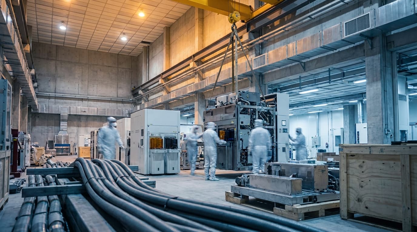
The shift is one of sequencing, not scope. Tool installation — moving in and qualifying the lithography, etch, and deposition equipment that turns a building into a working fab — is the gating step between construction and output. Pulling that into Q3 2026 puts N3 volume production on track for 2027 rather than 2028. Some reporting frames the ramp more precisely: main production lines installed in the first half of 2027, with volume output building in the second half of the year.
An important caveat for anyone underwriting capacity off these dates: these are reports, and not every detail has been formally confirmed by TSMC. The direction — earlier — is well-sourced; the exact month-by-month cadence is not contractual.
The $165B, six-fab program
The acceleration sits inside a much larger commitment. In March 2025, TSMC added $100 billion to its prior $65 billion Arizona pledge, bringing the announced total to $165 billion — described as the largest greenfield foreign direct investment in U.S. history and documented in the company's Form 6-K filing with the SEC. That figure expanded the planned footprint from three fabs to six, plus two advanced-packaging facilities and an R&D center.
The node roadmap is staggered across the campus:
-
Fab 1 is already in volume production on N4/4nm, ramping from late 2024 into early 2025.
-
Fab 2 is the subject of the acceleration — N3/3nm, now targeting 2027.
-
Fab 3 broke ground in late April 2025 near 43rd Avenue and Dove Valley Road, slated for N2 (2nm) and A16 (a 1.6nm-class node) with production aimed at roughly 2028–2029, and reported to add about 6,000 jobs. The groundbreaking and node targeting are both on the record.
Read together, the program is an attempt to plant a self-reinforcing leading-edge cluster — fabrication plus advanced packaging plus research — rather than a single isolated plant.
A campus reality check
One number worth getting right: the core campus. TSMC's official Arizona page describes the site as over 1,100 acres (about 1,130), not the 2,000-acre figure that sometimes circulates. The larger numbers in coverage typically refer to the surrounding ~3,500-acre mixed-use development known as Halo Vista, plus a separately reported ~900-acre land purchase — adjacent real estate, not the fab campus itself. The distinction matters for anyone modeling expansion headroom: the production complex is dense and contiguous, while the broader land position is about the ecosystem and housing that a fab cluster of this size demands.
The tariff wildcard
Looming over the confirmed program is a far larger, far less certain figure. A proposed U.S.–Taiwan tariff arrangement — reported to cut Taiwan's tariff rate to roughly 15% — has been linked to a dramatic escalation in TSMC's U.S. footprint. eeNews Europe cites a potential Arizona spend rising toward $465 billion across as many as 11 fabs, while CNBC has reported a broader ~$250 billion Taiwan commitment to U.S. chipmaking tied to the deal.
Treat those numbers as proposals, not plans. As of early 2026, they are not confirmed by TSMC, and Taiwan-side coverage from Focus Taiwan notes officials remained mum on the larger tariff-linked figures. The confirmed $165B program is the operating reality; the $465B scenario is a negotiating headline that could reshape the roadmap if it firms up — or evaporate.
Why this matters for U.S. supply chains
For TSMC's largest U.S. customers — Apple, Nvidia, AMD — a hardened leading-edge anchor in Arizona changes the geography of risk. 3nm is the node behind today's premium mobile and AI silicon; producing it domestically, a year earlier than planned, shortens the distance between design and wafer for the companies driving the AI buildout. It does not eliminate concentration risk — advanced packaging, mature nodes, and much of the supply base still sit in Asia — but it moves a meaningful slice of the most strategically sensitive capacity onshore faster.
The bottlenecks the acceleration runs into
Pulling tool-install forward intensifies two well-known constraints on U.S. fab ramps.
Power. Leading-edge fabs are enormous electrical loads. TSMC's two new Arizona facilities are reported to require nearly 200 MW of electricity — a figure cited alongside TSMC's work to cut EUV tool peak power. Bringing Fab 2 online sooner pulls that demand into the grid earlier, compressing the window utilities have to deliver firm capacity in a fast-growing metro that is also absorbing data-center load.
Labor and cost. TSMC has stated that U.S. construction costs run four to five times those of an identical plant in Taiwan, and it has sent U.S. workers to Taiwan for 12–18 months of training because qualified personnel were hard to find domestically. An accelerated tool-install schedule needs that trained workforce in place sooner — installing and qualifying equipment is precisely the labor-intensive, expertise-heavy phase where the skills gap bites hardest.
What to watch
Three markers will tell operators and investors whether the pulled-forward timeline holds. First, whether the larger tariff-linked figures (~$465B, ~11 fabs) get confirmed, scaled back, or quietly dropped — that determines the program's ceiling. Second, concrete Fab 2 ramp milestones through 2026 and into 2027: tool move-in, first wafers, and qualified yield. Third, grid and labor readiness — whether utility capacity and the Taiwan-trained workforce arrive on the compressed schedule, or whether power and people become the limiting reagents they have been at every prior U.S. leading-edge ramp.
Related reading
-
Micron's Manassas 1α DRAM Start Gives the U.S. a Third Memory Geography
-
The U.S. Trade Chief Just Sequenced Chip Tariffs — Memory and Mature Nodes Are the Exposed Surface
Sources
-
Tom's Hardware — TSMC brings its most advanced chipmaking node to the US yet
-
ABC15 — TSMC accelerates production timeline for new Arizona factory, reports say
-
TSMC — Intends to Expand Its Investment in the United States to US$165 Billion
-
azfamily — TSMC breaks ground on third facility in north Phoenix
-
SemiWiki — TSMC Arizona third-factory groundbreaking and N2/A16 targeting
-
eeNews Europe — TSMC Arizona expansion plan jumps to $465bn under proposed US–Taiwan tariff deal
-
NBC News — Trump administration reaches a trade deal to lower Taiwan's tariff barriers
-
CNBC — Taiwan will invest $250 billion in U.S. chipmaking under new trade deal
-
Focus Taiwan — Cabinet mum on possible U.S. tariff deal involving TSMC investment
-
Tom's Hardware — TSMC reduces peak power consumption of EUV tools by 44%