Speaking on May 22 at Micron's Manassas, Virginia memory fab — where the company has just begun 1α DRAM wafer production — U.S. Trade Representative Jamieson Greer told reporters there are no immediate semiconductor tariffs on the table, but that duties remain important to protect the sector and must be "properly sequenced" to promote U.S. output. The framing matters more than the timing: chip tariffs are not paused, they are queued.
For manufacturers buying chips into bills of materials — automotive, industrial controls, defense, medical devices, power electronics — the implication is that the Section 232 case that already bit advanced AI logic in January is going to bite somewhere else next. The two surfaces most exposed to a Phase 2 are the ones the administration deliberately left out of round one: memory and mature/legacy nodes.
What Section 232 already did — and what it skipped
The Presidential Proclamation of January 14, 2026, effective the next day, imposed a 25% Section 232 tariff on a narrow set of advanced logic chips — specifically articles falling under HTS 8471.50, 8471.80 and 8473.30 that meet Tensor Processing Performance and DRAM-bandwidth thresholds. In practice that means NVIDIA H200- and AMD MI325X-class accelerators, as parsed by trade counsel and confirmed by EY's tax-news desk.
Memory and mature/legacy-node logic were excluded by design. Commerce's underlying Section 232 report explicitly contemplated a Phase 2 of "significant" broader semiconductor tariffs after trade negotiations, and the proclamation itself requires the President to receive a market update by July 1, 2026 to consider modifications. Greer's May 22 remarks — independently reported by Reuters and Bloomberg — are best read as a Phase 2 trial balloon ahead of that review window.
Memory is the most exposed surface
The memory market is structurally tight in 2026. High-bandwidth memory (HBM) and high-capacity DDR5 for AI data centers are absorbing wafer capacity at every major supplier, leaving commodity DRAM and consumer-grade NAND undersupplied. Tesla, Apple and other major OEMs have publicly signaled that DRAM shortages will constrain 2026 production — and that is before any tariff layer hits.
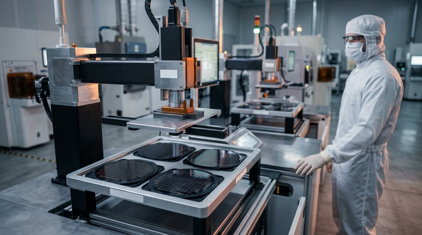
The reshoring math does not close in 2026 either. As the American Enterprise Institute has argued, a new commodity-DRAM fab starting construction today would not reach volume production until roughly 2028, given 18-to-24 months of construction plus ramp. Micron's Manassas 1α DRAM start in May 2026 is the most advanced memory node produced in the U.S. — backed by a $275 million CHIPS Act direct funding award and more than $2 billion of Virginia investment — but it is a single node at a single site, with end-markets in automotive, industrial, defense and medical applications.
That is the geometry of a tariff lever: domestic capacity is being built, but slowly enough that duties become the more responsive tool to push reshoring economics.
Mature nodes: rising China share, broken visibility
Legacy and mature-node chips — commonly defined as roughly 22–28 nanometers and older — are the other exposed surface. Congressional Research Service analysis puts China's share of global mature-node production at roughly 31% at the end of 2023, up from 17% in 2015, with TrendForce projecting about 39% by 2027. Those chips show up across automotive electronics, industrial controls, defense systems, medical devices, power applications and communications gear.
The harder problem is visibility. A January 2025 assessment by the Bureau of Industry and Security found about half of surveyed U.S. companies could not determine whether their products contained chips made in PRC foundries. As the Rhodium Group has documented, that traceability gap directly limits the precision of any tariff response — and means BOM-level exposure modeling has to start now, not after a proclamation lands.
The tariff stack manufacturers already pay
Any Phase 2 Section 232 duty would layer on top of an already-stacked regime on Chinese-origin semiconductors. The Section 301 rate on Chinese-origin chips moved to 50% on January 1, 2025, doubled from 25%. On December 23, 2025, USTR added a new Section 301 affirmative determination with an initial 0% rate that ramps on June 23, 2027 to a rate yet to be announced — confirmed in plain language by CBS News reporting on the deferred enforcement.
Translated to BOM math: a Chinese-origin mature-node chip already carries 50% Section 301. A Phase 2 Section 232 broadening to mature nodes or memory would compound on that base regardless of origin country, hitting Taiwanese, South Korean and Japanese supply too unless excluded by trade-deal carve-outs.
The carrot side of the policy stack
The reshoring subsidies are real, but they were not allocated evenly. According to CRS, CHIPS Act financial incentives directed roughly $28 billion (about 75%) to leading-edge logic and memory, and only about $10 billion (around 25%) to mature/current-generation and specialty production — with a specific $2 billion carve-out for mature semiconductors essential to military, automotive and manufacturing applications. That allocation is the structural reason mature nodes remain under-subsidized and tariff-exposed.
The leading-edge announcements continue to land. Micron's $200 billion U.S. plan — $150 billion of manufacturing and $50 billion of R&D, expanded by $30 billion in June 2025 — anchors memory reshoring across Idaho, New York and Virginia, with the Manassas 1α start confirmed in trade press. TSMC Arizona sits at more than $165 billion of announced investment, backed by $6.6 billion of CHIPS grants and up to $5 billion of loan guarantees; April 2026 reporting indicated consideration of up to 12 fabs and four advanced packaging facilities under a broader U.S.–Taiwan framework, and TSMC's board approved an up-to-$20 billion capital injection to TSMC Arizona on May 12, 2026.
The cliff in this stack is fiscal: the 25% advanced-manufacturing investment tax credit — a load-bearing input to reshoring economics — expires December 31, 2026. That sunset sits inside the same window as the Section 232 Phase 2 timeline, which is why the policy lever increasingly has to come from tariffs if subsidies plateau.
Operator playbook: model exposure before the next proclamation
For procurement and quality leaders inside manufacturing firms, the actionable framing is straightforward: a Phase 2 duty, if it comes, will hit before any new domestic capacity is ready to absorb the demand. The work to do now is exposure modeling.
-
Segment BOMs by node class. Break out spend and unit volume by leading-edge logic (≤14 nm), mature/legacy logic (22–28 nm and ≥40 nm), DRAM, NAND and HBM. The Section 232 scope to date has been HTS-coded; classification by node is the precondition for any tariff modeling.
-
Resolve country-of-origin to the foundry level. The BIS finding that half of surveyed firms could not trace PRC-foundry content is the gap to close. Country-of-origin attestations from distributors and EMS partners need to push back to fab, not just to assembly site.
-
Run HTS-classification audits. The January 2026 proclamation targets specific HTS 8471.50 / 8471.80 / 8473.30 subheadings; any Phase 2 expansion will sit in adjacent codes. Misclassification on inbound shipments is the first line of avoidable exposure.
-
Evaluate FTZ and tariff-engineering options. Foreign-trade-zone admittance, drawback programs and product re-engineering to shift HTS classification all have lead times measured in months — start before a proclamation, not after.
-
Stress-test memory supply. With Tesla and Apple flagging DRAM constraint for 2026 production, any plan that assumes spot-market availability for commodity DRAM or NAND needs a second source and a pricing collar.
The dates that matter
Four dates frame the next eighteen months for any manufacturer with semiconductor content in its BOM:
-
July 1, 2026 — Commerce market update to the President; the formal trigger for Section 232 modifications.
-
December 31, 2026 — Advanced-manufacturing investment tax credit sunsets, removing 25% of the reshoring subsidy stack.
-
June 23, 2027 — Section 301 rate on Chinese-origin semiconductors ramps from its current 0% placeholder to a rate to be announced.
-
2028 — Earliest plausible volume production for any commodity-DRAM fab that starts construction today.
The policy stack is converging in a recognizable shape: subsidies are pulling leading-edge logic home, and tariffs are about to push memory and mature nodes. As Chris Miller's congressional testimony on foundational chips has argued, the downstream exposure is concentrated in exactly the industries — automotive, industrial, defense — that cannot easily reformulate their BOMs in the window between proclamation and enforcement. The time to model that exposure is before Greer's "sequencing" lands, not after.
Related reading
Sources
-
USTR Greer sees no immediate chip tariffs but says protection important for sector — Reuters, May 22, 2026
-
US Weighs Chip Tariffs to Spur Domestic Growth, Trade Chief Says — Bloomberg, May 22, 2026
-
Adjusting Imports of Semiconductors, Semiconductor Manufacturing Equipment, and Their Derivative Products — White House Presidential Action, January 2026
-
President Trump orders narrowly targeted 25% Section 232 tariff on certain advanced semiconductor articles — White & Case
-
US Section 232 proclamation imposes 25% tariff on certain semiconductors — EY Global Tax News
-
Notice of Action: China's Acts, Policies, and Practices Related to Targeting of the Semiconductor Industry — Federal Register, Dec 29, 2025
-
Trump administration says China's chip policies are unfair but will delay tariffs to 2027 — CBS News
-
Section 301 and China: Mature-Node Semiconductors — CRS IF12958
-
Thin Ice: U.S. Pathways to Regulating China-Sourced Legacy Chips — Rhodium Group
-
Virginia expansion advances memory made in the USA — Micron Technology
-
Micron Advances Made-in-America Memory with Manufacturing Expansion in Virginia — HPCwire
-
Micron Technology announces ~$200bn investment in semiconductor manufacturing and R&D — The Manufacturer
-
TSMC Arizona — NIST CHIPS Office
-
TSMC Form 6-K — Board Approval of up to US$20B Capital Injection to TSMC Arizona — SEC, May 12, 2026
-
Semiconductors and the CHIPS Act: The Global Context — CRS R47558
-
Financial Markets Are Sounding the Alarm on Memory Chips — AEI
-
Foundational Chips: China's Ambitions and Implications — Chris Miller written testimony