
On Oct. 8, 2026, GlobalFoundries (GF) announced a multi-year, $2 billion agreement to make silicon interposers for TSMC's CoWoS advanced packaging ecosystem at its fab in Malta, New York. Volume production is expected to start ramping in the first half of 2028. Most buyers haven't dealt with this part before, so we start with what it is.
Silicon interposer explained
A silicon interposer is a passive slab of silicon that a processor or AI accelerator and its high-bandwidth memory (HBM) stacks sit on side by side. It carries wiring far denser than an organic substrate can support, and through-silicon vias pass signals and power down to the package substrate below. Think of it as a wiring backplane made of silicon.
The interposer has no transistors doing compute. Its job is to connect things. Converge Digest puts it this way: "Silicon interposers provide high-density electrical connections between processors, accelerator chiplets, and high-bandwidth memory (HBM) stacks within advanced semiconductor packages."
Silicon is used instead of a conventional package laminate because of density. SemiWiki's Daniel Nenni writes that "the silicon interposer enables wiring densities far beyond what organic substrates can support, with metal line pitches in the low single-digit microns," and that "through-silicon vias pass signals and power vertically through the interposer, connecting it to the package substrate below." An AI accelerator has to move huge amounts of data to and from its memory stacks, and it needs that many short, fine wires to do it.
These parts can be large. On TSMC's CoWoS technology page, the company has described an interposer "larger than 2X-reticle size (or ~1,700mm2)" that integrates SoCs with more than four HBM2/HBM2E cubes. That figure comes from an earlier generation of the technology. It shows the scale involved and should not be read as today's ceiling.
Why deep-trench capacitors are the new piece
GF's announcement highlights one feature in particular. The company says it expects to "expand capacity at its Malta facility and establish the first U.S.-based source of silicon interposers supporting advanced packaging technologies, including embedded deep trench capacitor components."
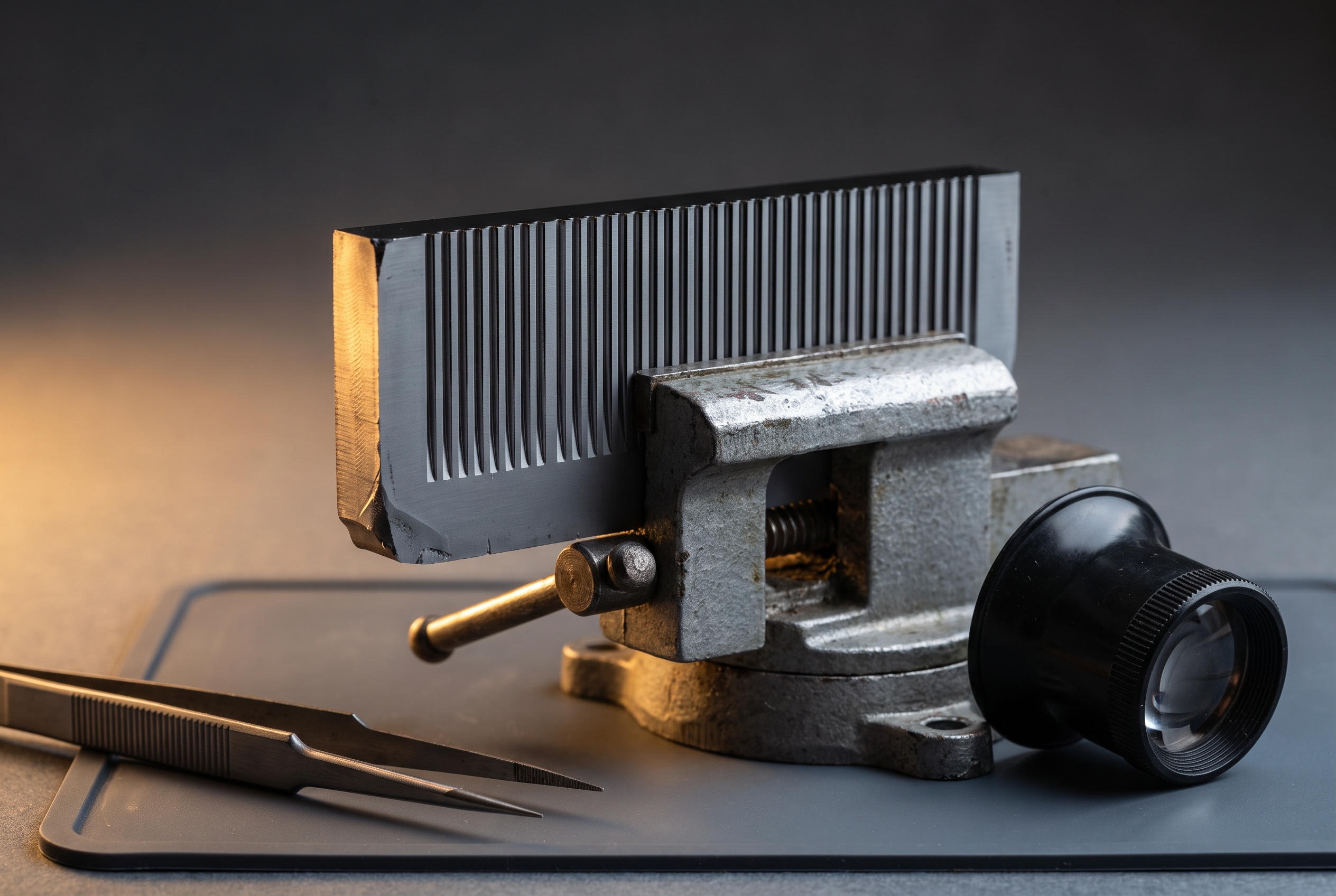
Deep-trench capacitors are built into the interposer itself. They store charge right next to the processor. Converge Digest explains: "Deep trench capacitors provide high-density capacitance within silicon structures. Integrating these components into interposers can help improve local power delivery and reduce voltage fluctuations associated with rapidly changing processor workloads." AI workloads can swing from idle to full load very quickly. Having charge stored a few microns from the die is part of what keeps the supply voltage stable through those swings.
The US did make interposers before this deal
The "first U.S.-based source" wording is easy to misread as "the US made no interposers before." That is wrong. In October 2024, Greg Kleese, GF's Aerospace and Defense Business Line Director, told 3D InCites that GF manufactures its 65PKG interposers in Malta and that the process is "production qualified, which is TRL9."
3D InCites reported the 65PKG specs at the time:
-
Three or four layers of 1.2 µm-thick copper
-
0.8 µm minimum critical dimension
-
1.6 µm vias between layers
-
10 µm x 100 µm through-silicon vias for signal, power and ground
In that 2024 article, deep-trench and MIM capacitors were listed only as future possibilities. The same piece pointed out that the US had historically had no production-volume sources of silicon interposers beyond prototypes: "in the U.S there just aren't any such sources." GF's 65PKG work had already begun to change that.
So the gap this deal fills is narrower and more precise: there was no US source of interposers compatible with TSMC's CoWoS ecosystem that also carry embedded deep-trench capacitors. The Deep Dive makes the same point in its headline: the deal builds on existing US interposer production.
Deal terms, and what was not disclosed
According to the GF press release:
-
Value: $2 billion, multi-year manufacturing agreement
-
Term: an initial five years, with a framework for future capacity expansion
-
Site: GF's fab in Malta, New York
-
Timing: volume production expected to begin ramping in the first half of 2028
The release quotes one person, Ed Kaste, senior vice president of CMOS Business at GF: "Advanced packaging is becoming increasingly critical to delivering the performance, power efficiency and scale required for next-generation AI systems. By providing manufacturing service using GF's trusted U.S. manufacturing footprint, we are creating a secure, scalable source of essential advanced-packaging elements that will help customers accelerate innovation and strengthen the semiconductor supply chain."
The release gives no job count and no capex figure. The Deep Dive reports that GF has not provided specifics on guaranteed purchase commitments, annual revenue, production volumes or capital expenditures. The forward-looking statements in the release mention funding GF has received, including awards under the US CHIPS and Science Act and New York State's Green CHIPS program, but they do not tie any specific award to this project. Read the $2 billion as a contract value. It does not tell you how much will be spent on tools or buildings in Malta.
The two companies already had ties. In November 2025, GF licensed TSMC's gallium nitride (GaN) technology.
Where Malta fits in the US packaging buildout
The interposer deal is one part of a larger domestic CoWoS supply chain that is coming together. In June 2026, TrendForce reported that TSMC and Amkor signed a 10-year agreement under which TSMC buys advanced packaging and test services from Amkor in Arizona. Amkor added 67 acres next to a 104-acre site in Peoria, with production slated to begin in 2028. The companies will jointly define technologies including InFO and CoWoS. TrendForce also reported that TSMC plans its first Arizona advanced-packaging facility, with CoWoS and 3D-IC capacity, by 2029.
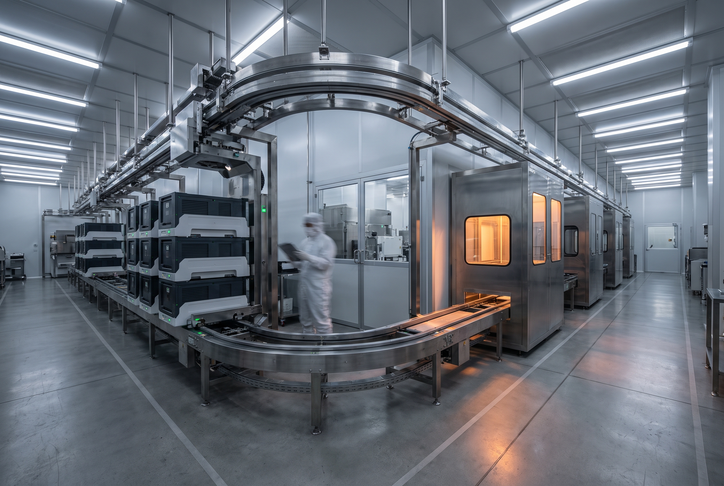
Taken together, the onshore CoWoS footprint for 2028 to 2029 looks like this: interposer manufacturing in New York, plus packaging, assembly and test in Arizona. Converge Digest notes that an advanced AI package needs much more than logic transistors: "high-quality interposers, fine-pitch interconnects, power delivery components, substrates, assembly, and testing." Until now the US had been missing several of those pieces at production scale.
What operators and suppliers should do with this
The points below are our analysis, not reported fact.
-
Plan around a 2028 window. The Malta ramp (first half of 2028) and Amkor Peoria's production start (2028) fall close together. Toolmakers, materials suppliers and service providers to wafer fabs and back-end packaging should look at sales capacity, field service staffing and qualification resources for that period, not for next year.
-
Put demand in the right state. Interposer manufacturing is a wafer-fab process, and it lands in New York. Substrate, assembly and test demand tied to this buildout sits mainly in Arizona. Suppliers that serve both front-end and back-end steps may need separate coverage plans for the two regions.
-
Do not budget off the headline. No capex, volume or purchase-commitment figures have been disclosed. Anyone building a forecast on Malta equipment demand is guessing until GF says more.
-
Track the right milestones. Converge Digest names the indicators that will show whether this program is real: qualification, early yields, interposer dimensions, supported packaging generations, and any expansion beyond the initial term. These are better progress signals than any follow-on announcement.
The bottleneck is moving to the package
For years the US chip debate centered on transistors and leading-edge fabs. AI accelerators have changed what is scarce. A top-end GPU is of no use without an interposer that can connect it to HBM, deliver clean power, and survive assembly. GF already makes production-qualified interposers in Malta. What the TSMC agreement adds is CoWoS compatibility and embedded deep-trench capacitors, in a fab within driving distance of a growing New York semiconductor corridor. The milestone to watch is GF's volume ramp in the first half of 2028. Until that happens, the US packaging gap is closing on paper, not yet on the line.
Related reading
Sources
-
Converge Digest: GlobalFoundries Signs $2B TSMC Deal for CoWoS Interposer Manufacturing
-
SemiWiki, Daniel Nenni: The Chronicle of TSMC CoWoS (Jan. 28, 2026)
-
TrendForce: TSMC, Amkor Sign 10-Year Arizona Advanced Packaging Pact (June 17, 2026)
-
GlobalFoundries investor release: GlobalFoundries Licenses GaN Technology from TSMC